
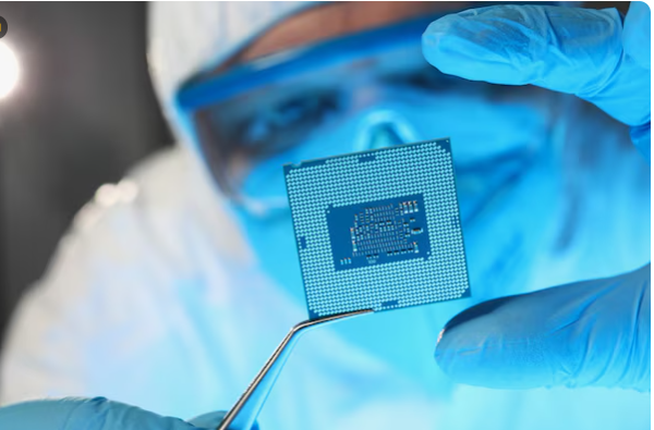

Faster AI chips, larger neural networks, and more intelligent processors are just a few of the astounding innovations that are frequently discussed at semiconductor conferences. Companies like NVIDIA, whose graphics processors power everything from chatbots to self-driving cars, are the ones making headlines. However, beneath the glamorous product releases and stage lights is a more subdued technology that many engineers claim is currently determining the destiny of the global chip race.
It doesn’t sound dramatic. In reality, rather than billion-dollar silicon wafers, the phrase might make you think of cardboard boxes. However, packaging has emerged as one of the most crucial and challenging phases in contemporary chipmaking across semiconductor plants from Taiwan to Arizona.
Key Information About Advanced Packaging in the Chip Industry
| Category | Information |
|---|---|
| Technology | Advanced Semiconductor Packaging |
| Key Purpose | Connecting multiple chip components into a single high-performance system |
| Major Companies | TSMC, Intel, NVIDIA |
| Critical Equipment | EUV lithography systems from ASML |
| Supporting Infrastructure | Semiconductor testing equipment from Teradyne |
| Industry Driver | Artificial intelligence and data-center chips |
| Bottleneck Issue | Manufacturing capacity and chip integration complexity |
| Reference Website | https://www.semiconductor.org |
It feels more like a hospital than a factory when you stand inside a chip production facility. Every movement is slow and deliberate, air filtering devices hum continuously, and workers wear complete protective suites. Engineers are working to find a solution to a problem that has subtly emerged as one of the defining challenges of contemporary computing, somewhere deep behind that meticulously managed maze of equipment.
How can dozens, or even hundreds, of tiny chip components be connected to function as a single brain?
Transistor shrinkage was the primary driver of semiconductor advancement for decades. More processing power was crammed into smaller areas with each successive generation of manufacturing technology. The entire digital revolution was propelled by this idea, which is frequently linked to Moore’s Law. However, something has altered.
The scaling of transistors is slowing down. Physics, it turns out, has limits. Although engineers are still able to reduce component size, the benefits are diminishing and the expenses are increasing significantly. This indicates that businesses have started looking for alternative methods to continue enhancing performance. Advanced packaging is becoming the solution.
Instead of creating a single large chip, manufacturers now put together systems that are composed of several smaller chips that cooperate. These chiplets are joined by extraordinarily thick networks of microscopic wiring and are arranged side by side or occasionally stacked vertically. The method seems straightforward. In reality, it’s quite difficult.
Consider TSMC, the massive Taiwanese company that makes many of the most cutting-edge semiconductors in the world. Its cutting-edge packaging technologies, such CoWoS and other connection systems, have all of a sudden emerged as one of the technology industry’s most valuable resources. Some AI companies apparently had to wait months to get packaging capacity due to the extreme demand.
The semiconductor tale has taken an unusual turn. Although the chips’ designs frequently draw attention, the packaging procedure that ties them together may be the factor that ultimately decides whether or not those designs make it to market. Even businesses that have historically been involved in chip creation are now vying to become experts in this neglected phase.
In order to put logic and memory closer together, Intel has made significant investments in its own packaging technologies, including as 3D stacking systems. By reducing the distance signals must travel, these systems increase speed and energy efficiency.
As engineers describe the process, it seems that creating chips is now more about coordinating large electronic ecosystems than it is about reducing the size of individual components. And packaging is the conductor.
Companies that are never brought up in popular conversations about artificial intelligence provide another important piece of this puzzle. Before sophisticated chips leave the manufacturing, companies like Teradyne construct the devices that check if they truly work. In the past, testing was commonplace. It’s a huge challenge now.
Several integrated chiplets and billions of transistors are found in contemporary AI processors. Once implemented in a data center, a single defect can result in catastrophic collapse. Testing systems need to advance in sophistication along with the complexity of semiconductor architectures. The machinery needed to produce the chips in the first place comes next.
Extreme ultraviolet lithography equipment, which can cost over $200 million apiece, are manufactured by the Dutch company ASML. These devices very precisely etch tiny circuits onto silicon wafers. The production of sophisticated chips would just stop without them.
It’s understandable why these technologies are at the center of growing geopolitical tensions. Governments are aware that having control over semiconductor infrastructure entails having an impact on defense systems, artificial intelligence, and economic competitiveness. Taiwan is in the middle of that precarious equilibrium.
Despite all the geopolitical drama, the true discoveries frequently take place in areas that few people ever see: silent cleanrooms where engineers discuss minuscule wiring designs, signal interference, and cooling systems. Seldom do these facts make news. However, they are quite important.
For instance, consider thermal management. AI processors produce incredible quantities of heat as they become more powerful. In order to prevent computers from overheating, direct liquid cooling systems—which occasionally require specialized polymer piping—have become crucial.
Even businesses known for their sophisticated product designs, like Apple, get technological benefits by focusing on these unglamorous details: signal paths, power efficiency, and component placement.
Engineers and investors alike are becoming increasingly aware of this as they watch the current semiconductor race. It’s possible that the future of computing will depend more on solving the quiet engineering challenges that keep things together than on spectacular discoveries.
